Direct detection of low-energy primary electron — a revolutionary advancement for LEEM/PEEM.
4k × 4k (16.8 million) pixels.
Movie-mode imaging of dynamic specimens with drift-correction.
DE Mission Control software saves open data fomats and is controllable by API.
The largest impact hardware upgrade you can make per dollar.
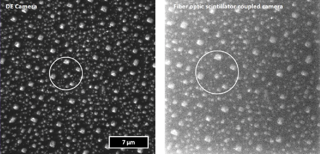
15keV comparison between the LV-16 (left) and a non-direct detection camera (right). The images show a silicon surface, collected in PEEM mode. The integration time was 300 seconds. The circle marks the same area in both images. The LV-16 was operated with 2x binning so that both images are 2k x 2k pixels. Courtesy of Rudolf Tromp, (IBM, Yorktown Heights, NY, USA).
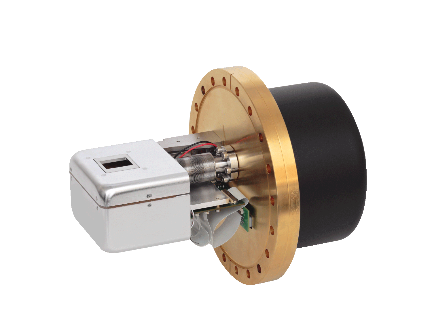
The LV-16 is the first and only commercially-available direct detection camera for low voltage electron microscopy. It features the 10th generation of our revolutionary Direct Detection Device (DDD®) sensor. In addition to dramatically better resolution and a larger field-of-view, the LV-16 also allows delivers full-frame unbinned streaming at up to 92 frames per second (fps) for motion correction or analysis of dynamics. For higher speeds, users acquire data at 281 fps with full-frame readout and 2×-binning, and substantially faster frame rates can be achieved by reducing the readout array size.
All of our LV-series cameras deliver state-of-the-art performance and unique features that make them ideal for a wide range of low voltage electron microscopy applications, including LEEM/PEEM. The LV-16 allows for direct detection of 10 – 40 keV primary electrons—a revolutionary advancement in data quality. Its improved resolution yields approximately 8× more information per image compared to MCP+CCD. Direct Electron’s patented “movie mode” provides high-speed acquisition of a continuous stream of frames with nearly 100% duty cycle and little to no dead time between frames. Specifically designed for low voltage applications to give you clear data at incredibly quick speeds.
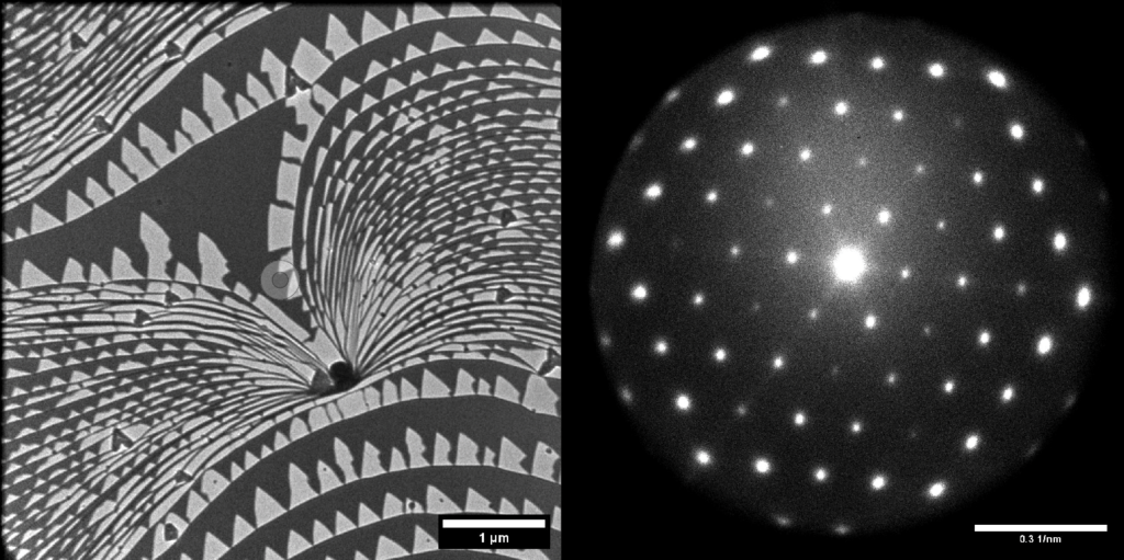
Left: image of Si(111), with (7×7) (bright) and (1×1) (dark) co-existing at about 860 Celsius, imaged in LEEM mode at 10.7 eV.
The dark spot is a carbide defect on the surface and the lines emanating from it are atomic steps.
Right: A LEED diffraction pattern of Si(111) acquired at 5.5 keV bounded by the edge of the Ewald sphere.
Diffraction spots are due to the (7×7) reconstruction.