PRODUCTS
NanoBiz Korea
NanoBiz Korea
Product Description
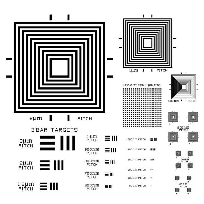
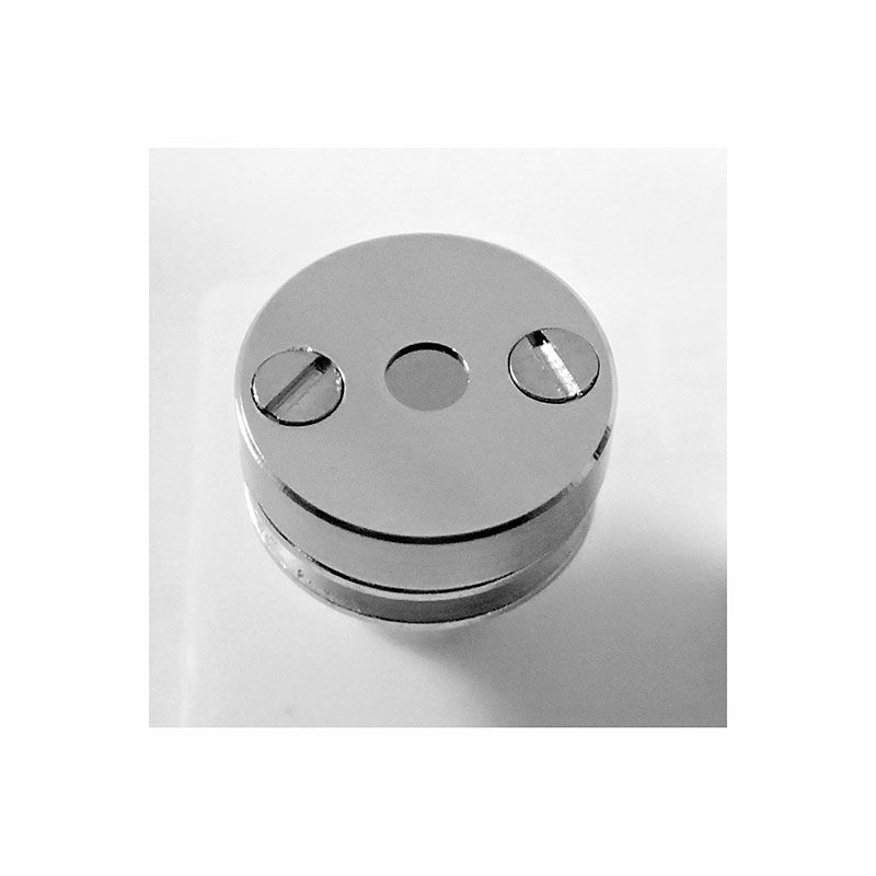
The MRS-6 is fabricated by using the highest accuracy electron direct write semiconductor manufacturing equipment available today. The pattern is built on a silicon wafer with ~15nm Cr film. This film, which is significantly thinner that that of the previous MRS-5, has superior edge quality. Imaging contrast in both secondary and backscattered electron mode is possible with field emission SEMs and newer tungsten or LaB6 SEMs. The overall size is ~ 3mm x 3mm x 0.25mm thick. The MRS-6 is fully conductive. No conductive coatings are necessary.
The MRS-6 has three types of pattern (the geometric design of the MRS-6 and previous MRS-5 are the same):
Typical applications include:
Technical Data MRS-6 Technical Datasheet
제품 | 제품 코드번호 |
MRS6 Geller Reference Standard Non Traceable | AGS1814 |
MRS6 Geller Reference Standard Non Traceable with Retainer Pin | AGS1814-P |
MRS6 Geller Reference Standard XY Traceable | AGS1815 |
MRS6 Geller Reference Standard XY Traceable with Retainer Pin | AGS1815-P |


