PRODUCTS
NanoBiz Korea
NanoBiz Korea
Product Description
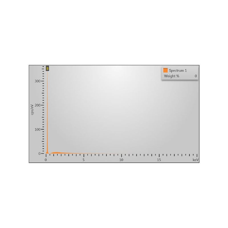
A considerable number of natural and artificial materials are made of light elements such as carbon (e.g. soot), nitrogen (e.g. nitrates) and oxygen (e.g. minerals). Advances in EDX technology enable measurement and semi-quantitative determination of light elements in micro and nano-materials using SEM. Traditionally carbon tabs and polycarbonate filters are used as substrates or sampling surfaces for subsequent SEM/EDX analysis. The disadvantage of these carbon bearing substrates is the carbon concentration cannot be determined for particles smaller than 2μm in diameter or for materials built of thin structures. The evaluated carbon is not only from the analysed substance but also from the substrate itself.
This development of boron substrates combined with state-of-the-art, high-resolution EDS systems it is now possible to analyse carbon and other light elements semi-quantitatively. This progress applies to both manual and fully automated SEM/EDX analysis.
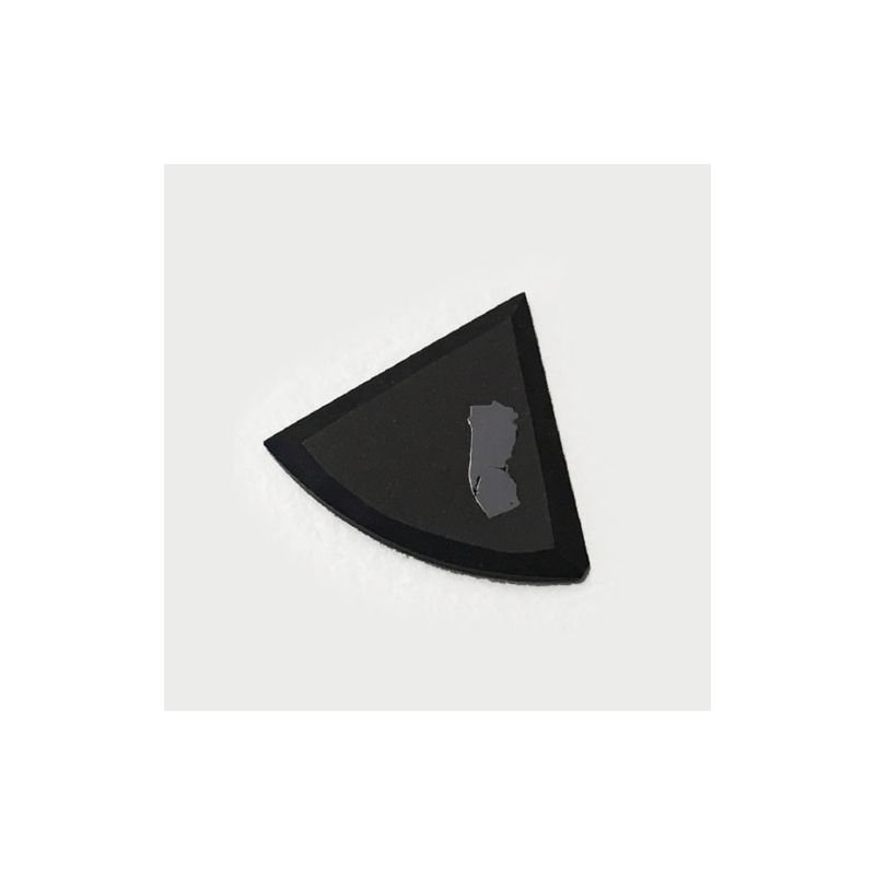
All substrates carry an individual serial number. To improve the sample application, the substrate but can also be provided with a very thin based acrylic based adhesive layer.
Four types are available:
● AGS310 - Standard Boron surface approx. 1mm² on a 1cm² triangle substrate,
without adhesive
● AGS311 - Standard Boron surface approx. 1mm² on a 1cm² triangle substrate,
with adhesive
● AGS320 - Premium Boron, surface approx. 2mm² on a 1cm² triangle substrate,
without adhesive
● AGS321 - Premium Boron surface approx. 2mm² on a 1cm² triangle substrate,
with adhesive

Features & Specifications;
제품 | 제품 코드번호 |
Boron surface for SEM/EDX, ca. 1mm² on 1cm² triangle, no adhesive (Standard) | AGS310 |
Boron surface for SEM/EDX, ca. 1mm² on 1cm² triangle, with adhesive (Standard) | AGS311 |
Boron surface for SEM/EDX, ca. 2mm² on 1cm² triangle, no adhesive (Premium) | AGS320 |
Boron surface for SEM/EDX, ca. 2mm² on 1cm² triangle, with adhesive (Premium | AGS321 |


