PRODUCTS
NanoBiz Korea
NanoBiz Korea
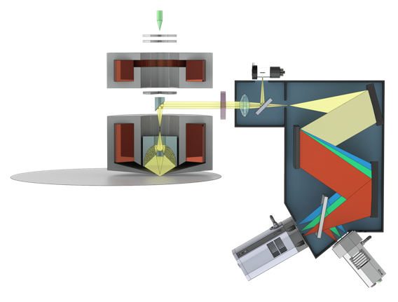
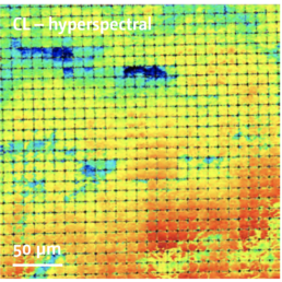
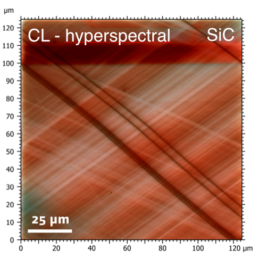
Attolight’s Quantitative CL-SEMs offer “No Compromise” large field fast scanning simultaneous acquisition of SEM image, hyperspectral CL maps, and optical spectra.
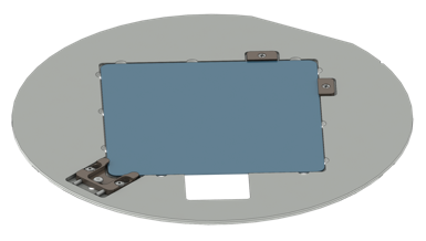
Smaller diameter wafers, or miscellaneously shaped substrates are manually loaded on intermediary 300mm susceptors subsequently handled automatically by the tool.
The Santis 300 system offers 3 distinct acquisition modes: step and repeat (S&R), continuous scanning mode (AWpix), integrative scanning mode (FWbrush)
Various system configurations are available, the system is fully upgradeable from P1 to P3:
The Attolight Quantitative Cathodoluminescence comprises a custom designed electron column with tightly integrated light collection optics.
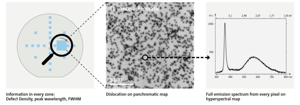
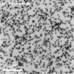
The light collection optics featured a field of view of up to 300 μm. The light detection path is carefully optimized and fully aperture matched to guarantee highest light collection uniformity (+-1%) over the FOV. The carefully integrated design and optimization of light and electron optics make high measurement speeds, accuracy and repeatability possible. Quantitative CL produces UV-Visible and NIR hyperspectral maps (full emission spectrum in every pixel) or panchromatic maps (intensity of defined wavelength in every pixel).
Attolight Säntis 300 system offers 3 distinctive acquisition modes, tailored for different needs and applications:
Step and repeat
Traditional frozen mapping allowing repetitive acquisitions at fixed locations spread over the wafer. Measurements and analysis parameters can be defined and stored in a recipe database.
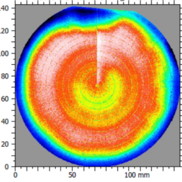
Innovative full measurement of the wafer area allowing medium resolution imaging of the whole wafer. Partial wafer imaging possible. Measurements and analysis parameters can be defined and stored in a recipe database.
Down to 0.1 µsec per pixel (intensity at given wavelength)
0.5 to 2.5 µm pixel Simultaneous SE image
< 2.5 h per wafer for 100 % coverage of a 150 mm diameter wafer
Innovative high speed measurement of the wafer area allowing low resolution imaging of the whole wafer. Partial wafer imaging possible. Measurements and analysis parameters can be defined and stored in a recipe database
Down to 0.1 µsec per pixel (intensity at given wavelength) Down to 1 msec per pixel (Full spectra)
300 µm pixel Simultaneous SE image
Up to 4 wafers per hour for 100% coverage of 150 mm diameter wafers
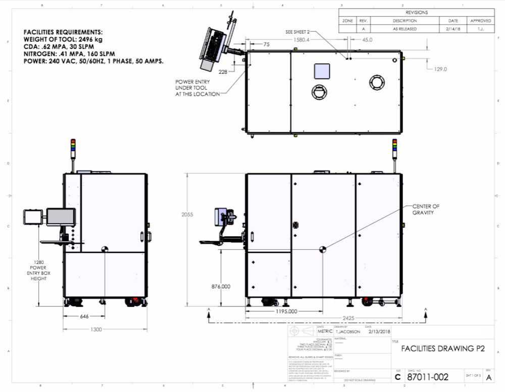
Tool weight :
Facilities :
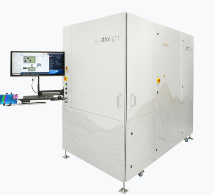
Operator manually loading wafer into the loadlock of a Säntis 300 P2 tool